AMD (formerly Xilinx) FPGAs: Part 2 Synthesis and testing on device
Introduction
In the previous tutorial, you ran through the automated simulation of a full adder. In this section, you will learn how to synthesize the full adder and run tests on the FPGA device using the Integrated Logic Analyzer (ILA) IP core.
You can find the source code for this example here.
Creating and running a hardware testbench
Creating a block diagram
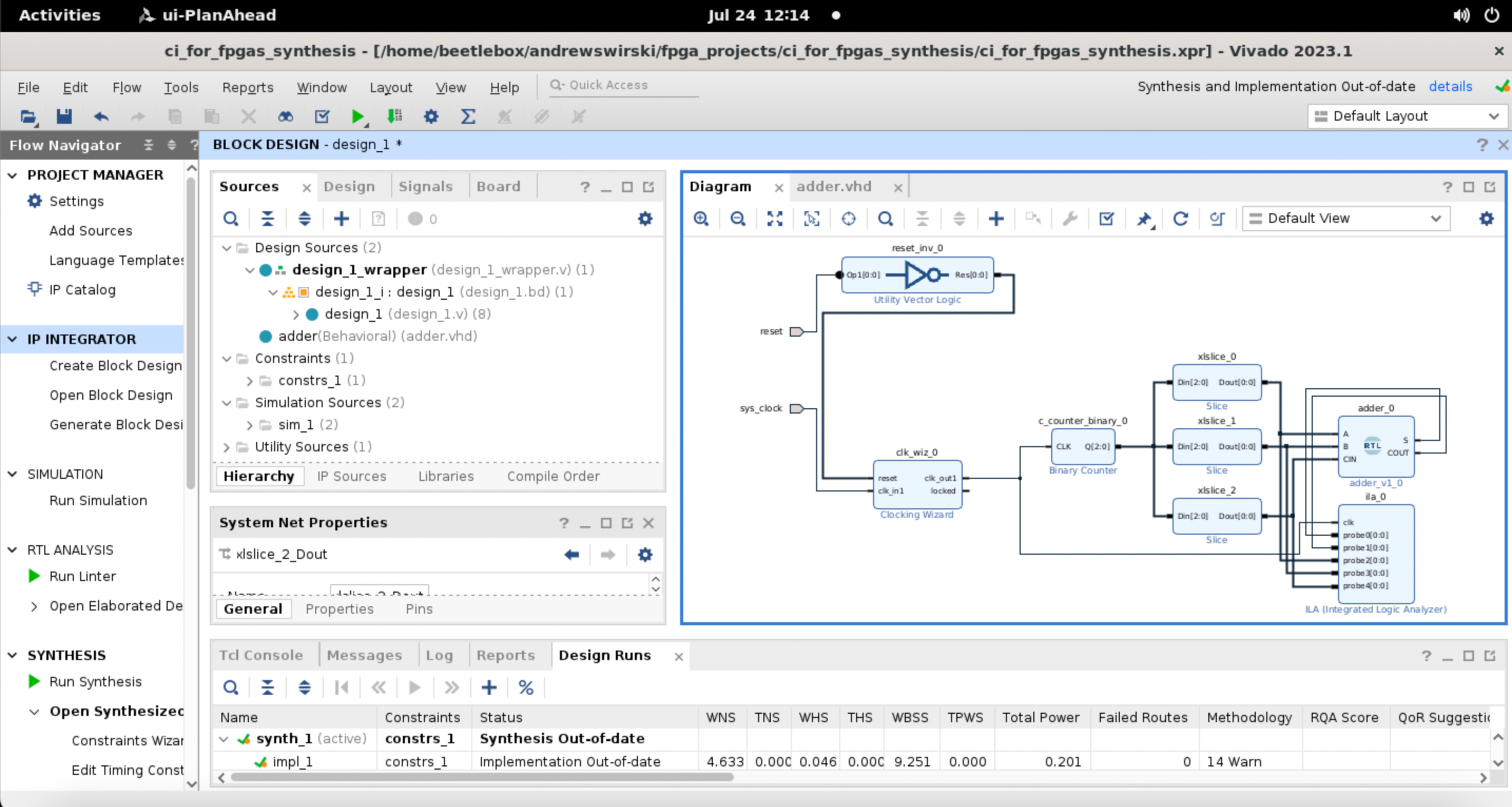
The testbench you created previously is not synthesizable for your FPGA. To test on actual hardware, you need to create a hardware testbench by including IP that can stimulate the full adder's input and then use the ILA core to record the waveforms. The first step is to create a block diagram of our design.
- In Vivado, in the
Flow Navigator, selectCreate block diagramunderIP Integrator. TheCreate Block Designwindow will open. SelectOK. - The
BLOCK DESIGNtab will now open. UnderSources, findDesign Sourcesand then right clickadder. Then selectAdd module to Block Diagram, which will add your full adder to the block diagram.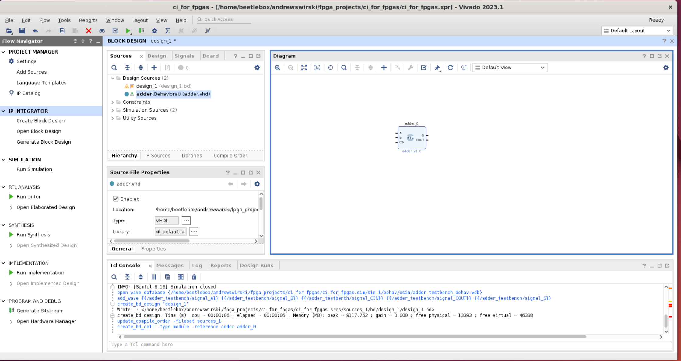
- Now you need a clock source. Right click the block diagram and select
Add IPthen find theClocking WizardIP. - A message on the block diagram stating
Designer Assistance Available. Run Connection Automationshould appear. SelectRun Connection Automation. In the newRun Connection Automationwindow, selectAll Automation.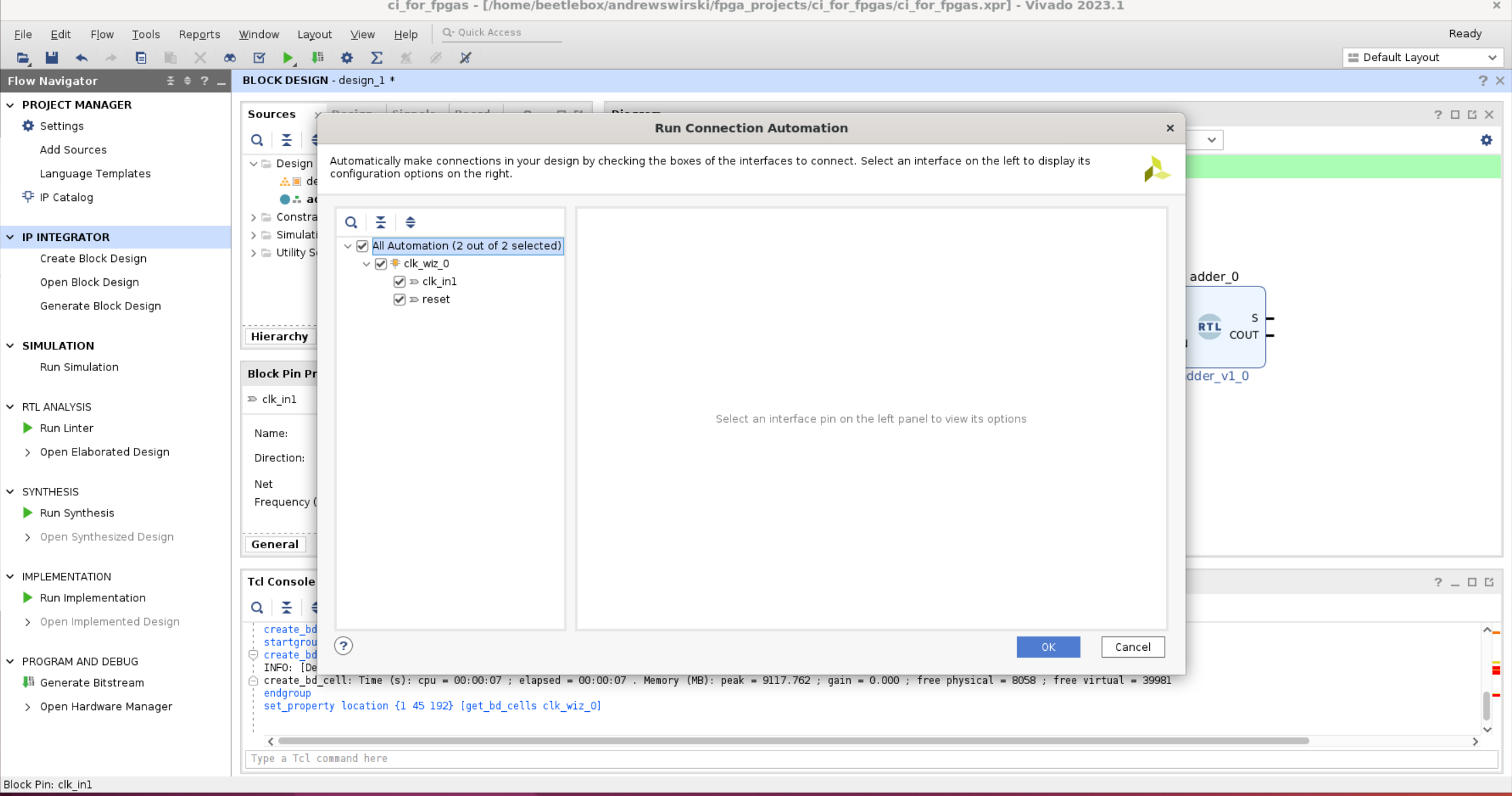 This will automatically connect a
 sys_clockand aresetpin to the block diagram.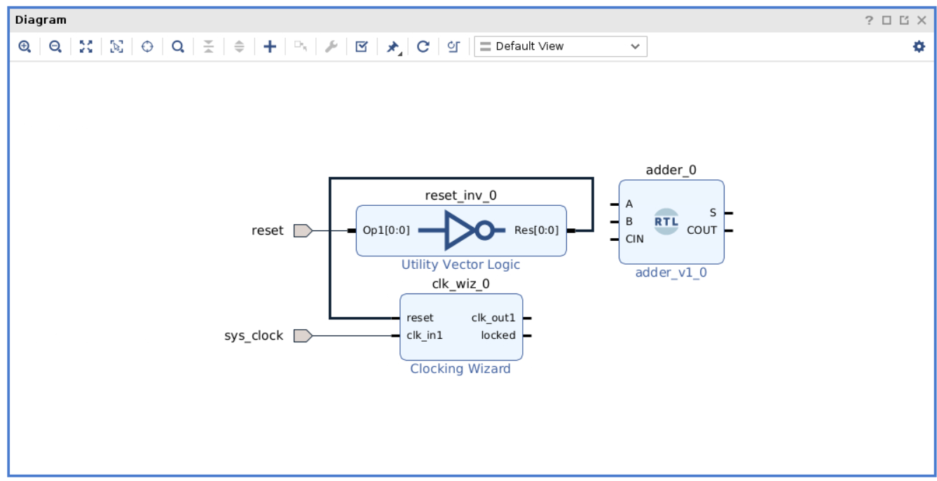
- To write to your adder inputs, you will use a simple 3-bit counter. Right click the block diagram and select
Add IPthen find theBinary CounterIP. - Double click the
Binary Counterto open up theRe-customize IPwindow and modify theOutput Widthto be3. - Connect the
CLKof theBinary Countertoclk_out1of theclk_wiz_0. - Add three
SliceIPs. Modify each one as follows:- xlslice_0 Din Width: 3, Din From: 0, Din Down To: 0, Dout Width: 0
- xlslice_1 Din Width: 3, Din From: 1, Din Down To: 1, Dout Width: 0
- xlslice_2 Din Width: 3, Din From: 2, Din Down To: 2, Dout Width: 0
- Connect the input of each
Sliceto the output of theBinary Counter. - Connect each
Sliceoutput as follows:- xlslice_0: Dout[0:0] -> A
- xlslice_1: Dout[0:0] -> B
- xlslice_2: Dout[0:0] -> Cin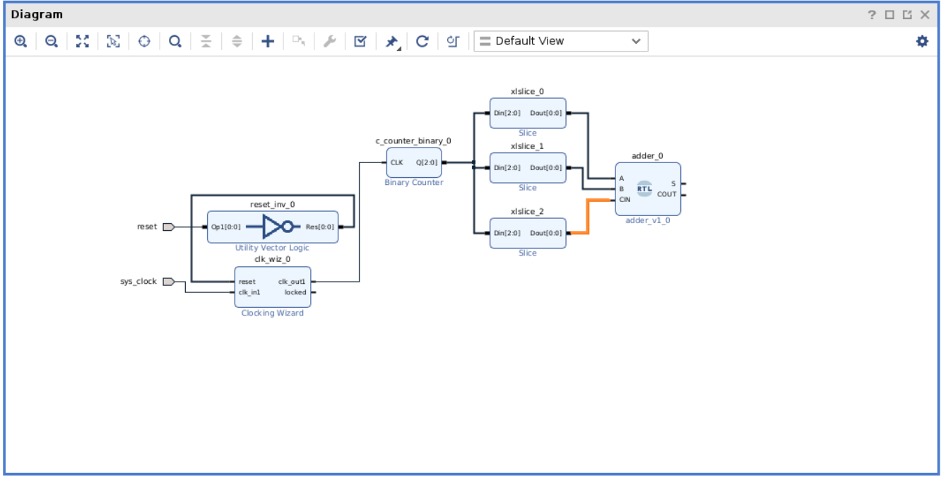
- Now you need to add the ILA. Right-click the block diagram and select
Add IPthen find theILAIP. - Double click the ILA to customize it. Change
Monitor TypetoNativeandNumber of Probesto5. - Attach the ILA input port
clktoclk_out1of theclk_wiz_0. - Attach the ILA input port
probe0[0:0]toSof theadder_0. - Attach the ILA input port
probe1[0:0]toCOUTof theadder_0. - Attach the ILA input port
probe2[0:0]toAof theadder_0. - Attach the ILA input port
probe3[0:0]toBof theadder_0. - Attach the ILA input port
probe4[0:0]toCINof theadder_0.
 19. Right-click the block diagram and select
 Validate Design. Vivado should indicate that validation was successful.
20. Under Flow Navigator and the IP INTEGRATOR section, select Generate Block Design. Wait for the block design to successfully generate.
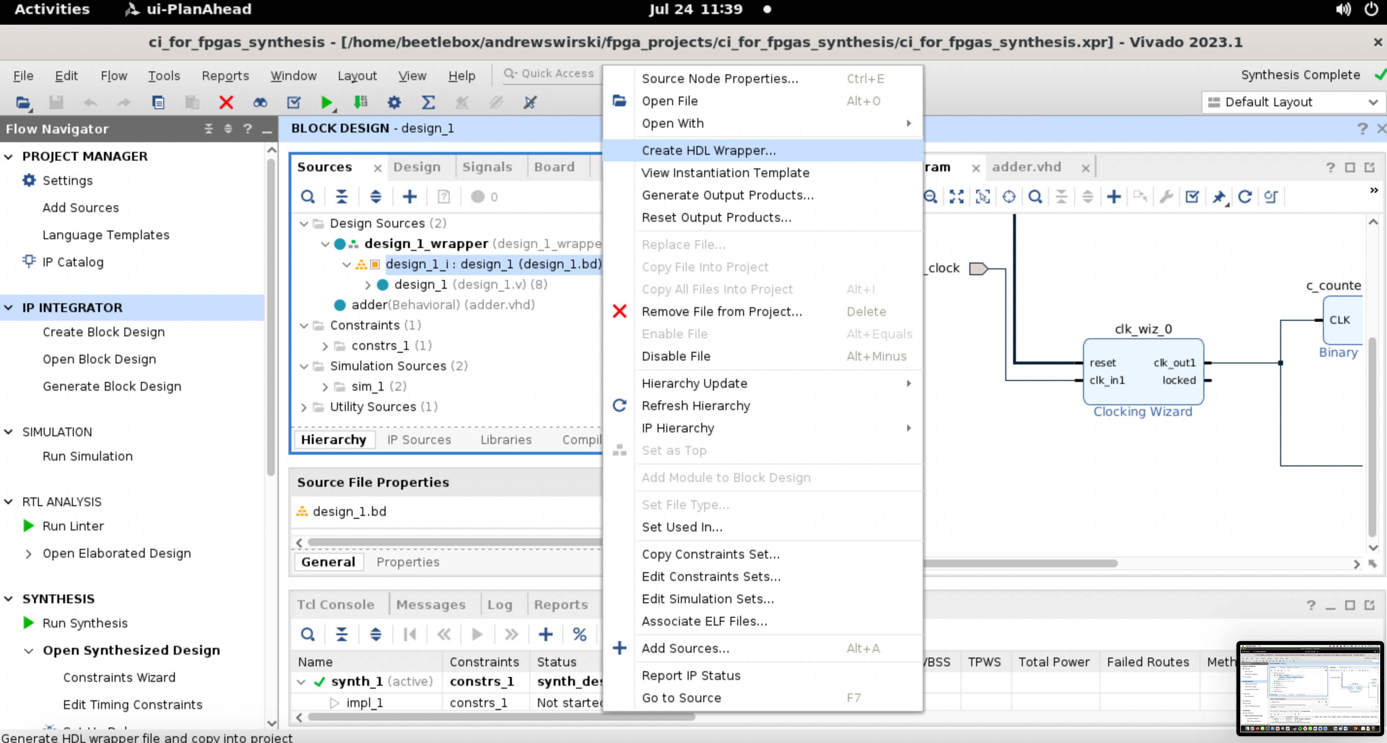
21. Back in the BLOCK DESIGN, under Design Sources, right-click design_1.bd and select Create HDL Wrapper.... In the Create HDL Wrapper window, select Let Vivado manage wrapper and auto-update, then select OK.
 22. Right-click the generated HDL and select
 Set as Top.
23. Under Flow Navigator and the PROGRAM AND DEBUG section, select Generate Bitstream. This will open the Save Project window to which you should select Save. The Launch Run window should now open and you can select OK. After a while, you should receive a success message. Select Open Hardware Manager.
Running the hardware testbench
Now that you have generated your bitstream, you can run your hardware testbench. To do so, you need to program your device and then capture the results from the ILA.
In the Hardware Manager under
hardware, right-click your device, then selectProgram Device.... TheProgram Devicewindow should appear, where you can selectProgram.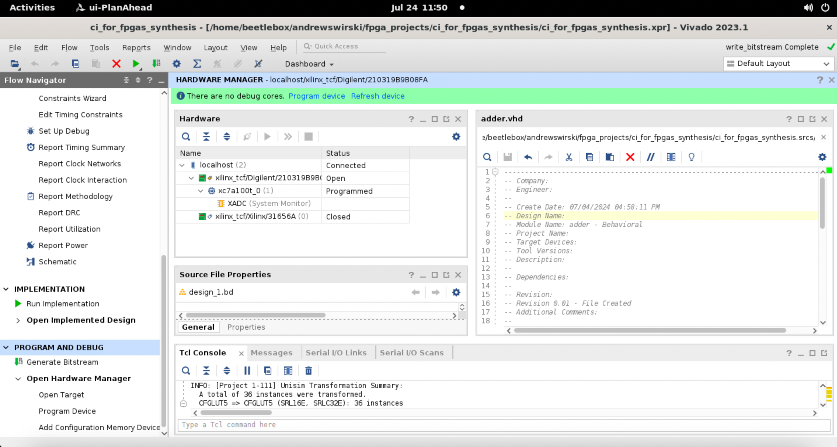
This should open your
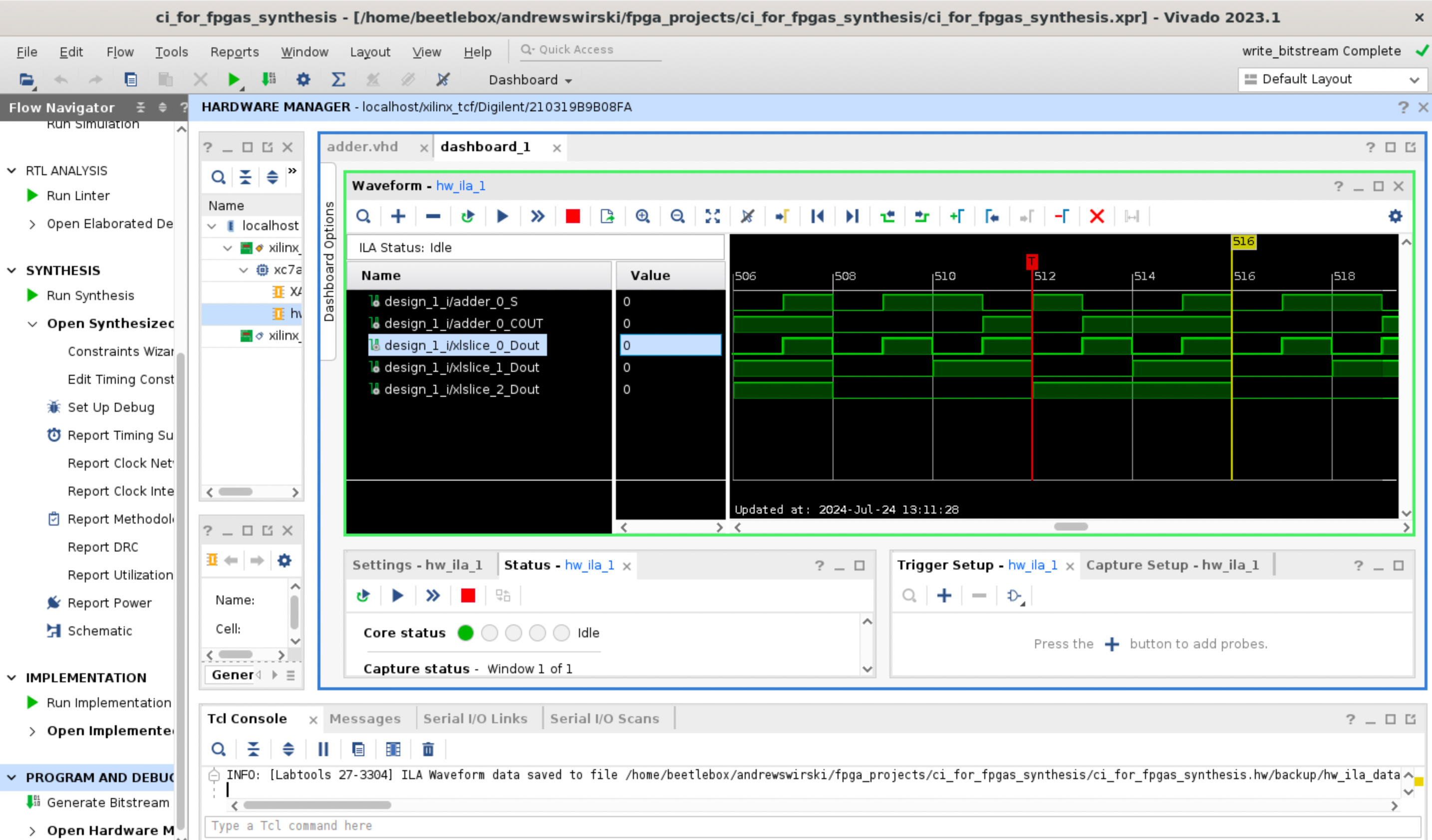
hw_ila_1waveform window. In theWaveformtab, select thePlaybutton.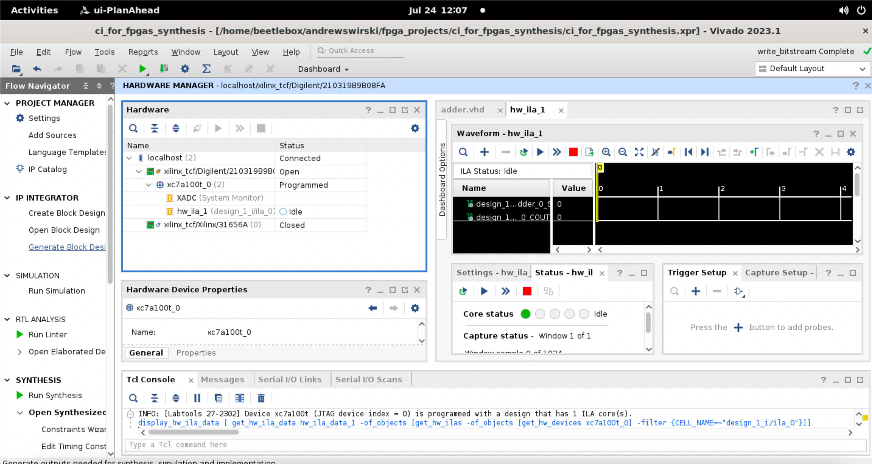
The ILA should then capture the waveforms running on the device itself!
Automating the hardware testbench to the repo
Adding the hardware testbench to the repo
Now that you have a working hardware testbench, you need to add it to the repository alongside the tcl files that are needed to synthesize the file, program the device, and trigger the ILA.
- You first need to update your
.gitignorefile to include the generated files. Make sure to push this to the repo:
# Blocklist files/folders in same directory as the .gitignore file
/*

# Includelist some files
!.gitignore
!README.md

# Include xpr and srcs
!ci_for_fpgas.srcs/
!ci_for_fpgas.srcs/*
!ci_for_fpgas.xpr

# Include gen files
!ci_for_fpgas.gen/
!ci_for_fpgas.gen/*

!tcl_scripts/
!tcl_scripts/*
- For automated runs you will also need to set the pins in the constraints. Create a constraints file, by going to the
Flow Navigatorand selectingAdd SourcesunderPROJECT MANAGER. Create one calledpin_constraints.xdcand copy in the following code:
set_property PACKAGE_PIN E3 [get_ports sys_clock]
set_property IOSTANDARD LVCMOS33 [get_ports sys_clock]
set_property PACKAGE_PIN C2 [get_ports reset]
set_property IOSTANDARD LVCMOS33 [get_ports reset]
If you are using a different board than the A7-100, you will need to change these pins to the relevant ones for your board. You can look in the pin planner to see what Vivado has automatically assigned to them.
- You are now going to add a tcl script for running through synthesis, implementation and bitstream generation. In your
tcl_scriptsfolder, add the followingrun_synthesis.tclfile:
open_project ci_for_fpgas.xpr
update_compile_order -fileset sources_1
reset_run impl_1 -prev_step
launch_runs impl_1 -to_step write_bitstream -jobs 4
- You also need a tcl script to program your board and trigger the ila. In your
tcl_scriptsfolder, add the followingprogram_device_trigger_ila.tclfile:
open_hw_manager
connect_hw_server -allow_non_jtag
open_hw_target
set_property PROBES.FILE {./ci_for_fpgas.runs/impl_1/design_1_wrapper.ltx} [get_hw_devices xc7a100t_0]
set_property FULL_PROBES.FILE {./ci_for_fpgas.runs/impl_1/design_1_wrapper.ltx} [get_hw_devices xc7a100t_0]
set_property PROGRAM.FILE {./ci_for_fpgas.runs/impl_1/design_1_wrapper.bit} [get_hw_devices xc7a100t_0]
program_hw_devices [get_hw_devices xc7a100t_0]
refresh_hw_device [lindex [get_hw_devices xc7a100t_0] 0]
run_hw_ila [get_hw_ilas -of_objects [get_hw_devices xc7a100t_0] -filter {CELL_NAME=~"design_1_i/ila_0"}]
wait_on_hw_ila [get_hw_ilas -of_objects [get_hw_devices xc7a100t_0] -filter {CELL_NAME=~"design_1_i/ila_0"}]
write_hw_ila_data {./iladata.ila} hw_ila_data_1
If you are using a different board than the A7-100, you will need to change xc7a100t_0 to the FPGA found on your board. You can find that out by looking at your hardware manager or by seeing the commands that are run by your tcl console in Vivado when you program the board.
5. Make sure to push all these files to your Git repo.
Running the pipeline
Now you have the files you need, you need to make a few modification to your config.yaml file then you will be ready to run the pipeline
- Modify your
config.yamlfile to add two more steps and new artifacts:
# Example config file to use as a starting point.
# Please visit https://docs.beetleboxci.com/docs/config/configuration-yaml for guidance on setting up your configuration file.

# Define a runner that will be used to run a job
runners:
 ubuntu-runner:
  image: public.ecr.aws/y2s4f3y9/ubuntu-generic

# Define a job to be performed during a workflow
jobs:
 run-sim-syn-job:
  # Specify the runner used to perform this job
  runner: ubuntu-runner
  resource_spec: large
  output:
   artifact:
    - ci_for_fpgas.sim/
    - ci_for_fpgas.hw/
    - ci_for_fpgas.runs/
    - ci_for_fpgas.cache/
    - iladata.ila
  volumes:
    - mount:
        name: volume1
        path: < The installation directory of Xilinx tools, by default this is /tools/Xilinx>

  # Define one or more steps to execute commands as part of the job
  steps:
   - run:
      name: Initalise vivado environment
      command: |
        apt-get update
        apt-get install locales
        locale
        locale-gen "en_US.UTF-8"
        update-locale LANG=en_US.UTF-8
   - run:
      name: Run Simulation
      command: |
        cd < The installation directory of Vivado, by default this is /tools/Xilinx/Vivado/2023.1/>
        source settings64.sh
        cd $HOME
        ls
        vivado -mode batch -source tcl_scripts/run_sim.tcl  | tee simulation_output.txt
   - run:
      name: Parse simulation for errors
      command: |
        # Path to the file to be checked
        FILE_PATH="./simulation_output.txt"
        # Check if the file exists
        if [[ ! -f "$FILE_PATH" ]]; then
         echo "File does not exist: $FILE_PATH"
          exit 1
        fi
        # Search for the phrase "Error: Assertion violation" in the file
        if grep -q "Error: Assertion violation" "$FILE_PATH"; then
          echo "Error: Assertion violation found in file."
          exit 1
        else
          echo "No assertion violations found. Passing."
          exit 0
        fi
   - run:
      name: Run Bitstream Generation
      command: |
        cd /tools/Xilinx/Vivado/2023.1/
        source settings64.sh
        cd $HOME
        vivado -mode batch -source tcl_scripts/run_gen_bitstream.tcl  | tee bit_stream_gen_output.txt
   - run:
      name: Program Device and Trigger ILA
      command: |
        cd /tools/Xilinx/Vivado/2023.1/
        source settings64.sh
        cd $HOME
        vivado -mode batch -source tcl_scripts/program_device_trigger_ila.tcl  | tee program_device_trigger_ila.txt

# Define a workflow to orchestrate a job
workflows:
 run-sim-syn-workflow:
  jobs:
   - run-sim-syn-job
The first new step Run Bitstream Generation runs through the synthesis, implementation and bitstream generation. Afterwards, Program Device and Trigger ILA will use that generated bitstream to program your device, trigger the ILA and capture the waveforms. You will also notice the new line resource_spec: large. This provides 16GB of memory which is needed for synthesis runs.
  output:
   artifact:
    - ci_for_fpgas.sim/
    - ci_for_fpgas.hw/
    - ci_for_fpgas.runs/
    - ci_for_fpgas.cache/
    - iladata.ila
Finally, you also include some new folders that will allow you to access the files generated for this build, so the artifact output is also modified. You will also need the iladata.ila file to check the results of the testbench.
- Go back to BeetleboxCI and run the new pipeline. On the job page, it should be successful and show the following:
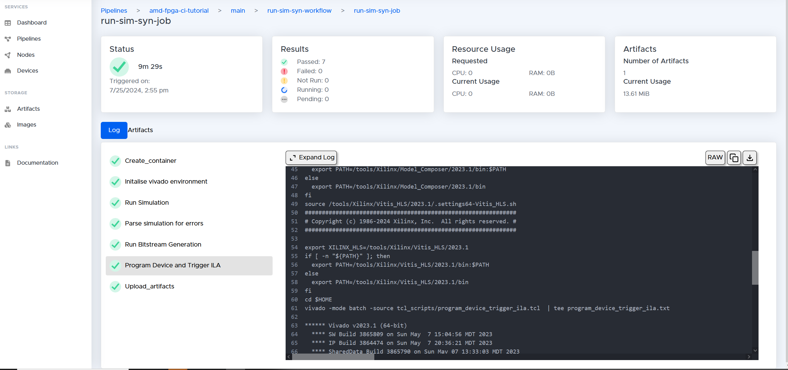
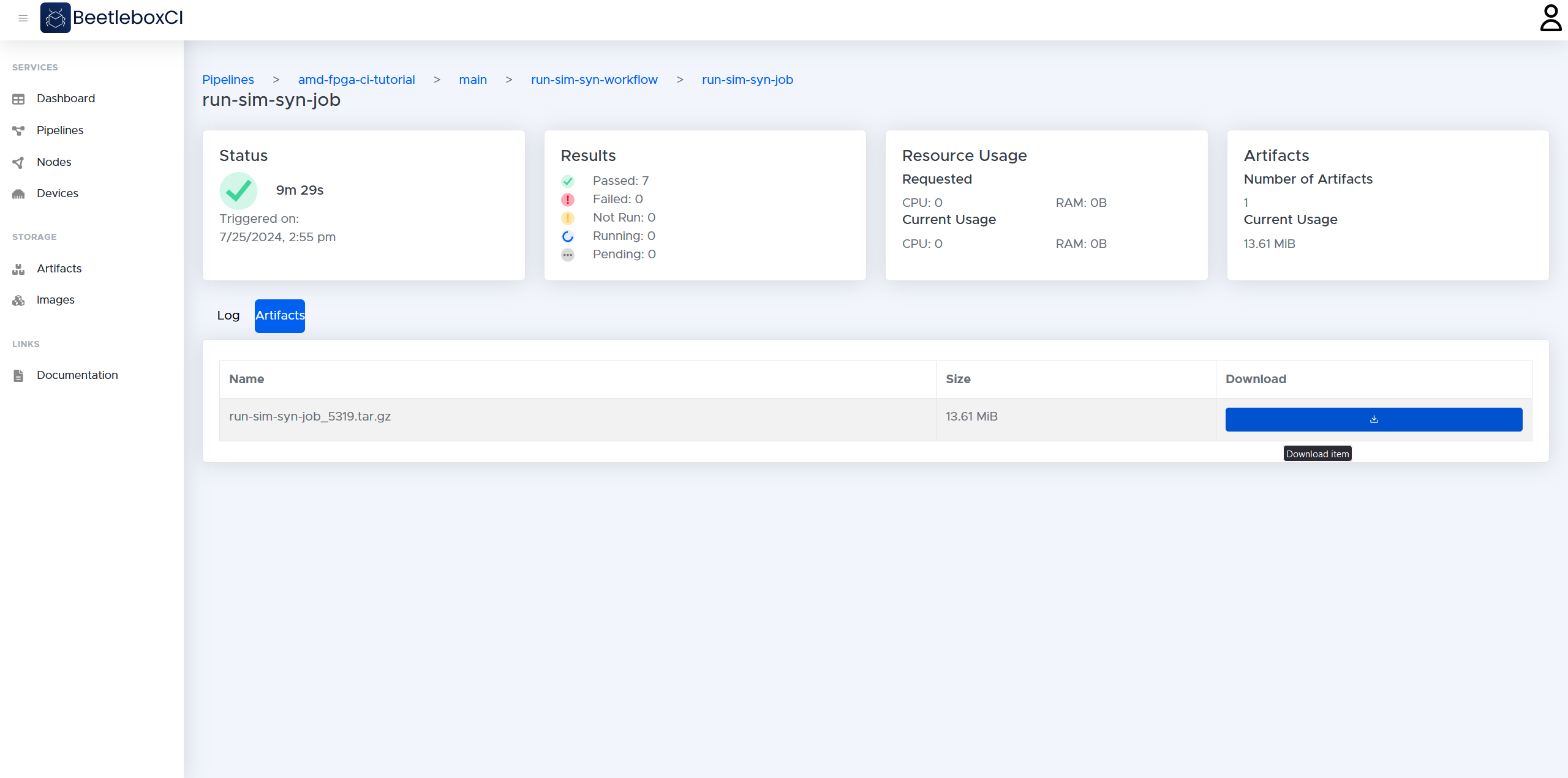
- On the job page, go the
Artifactstab and download the compressed folder that contains all the artifacts:
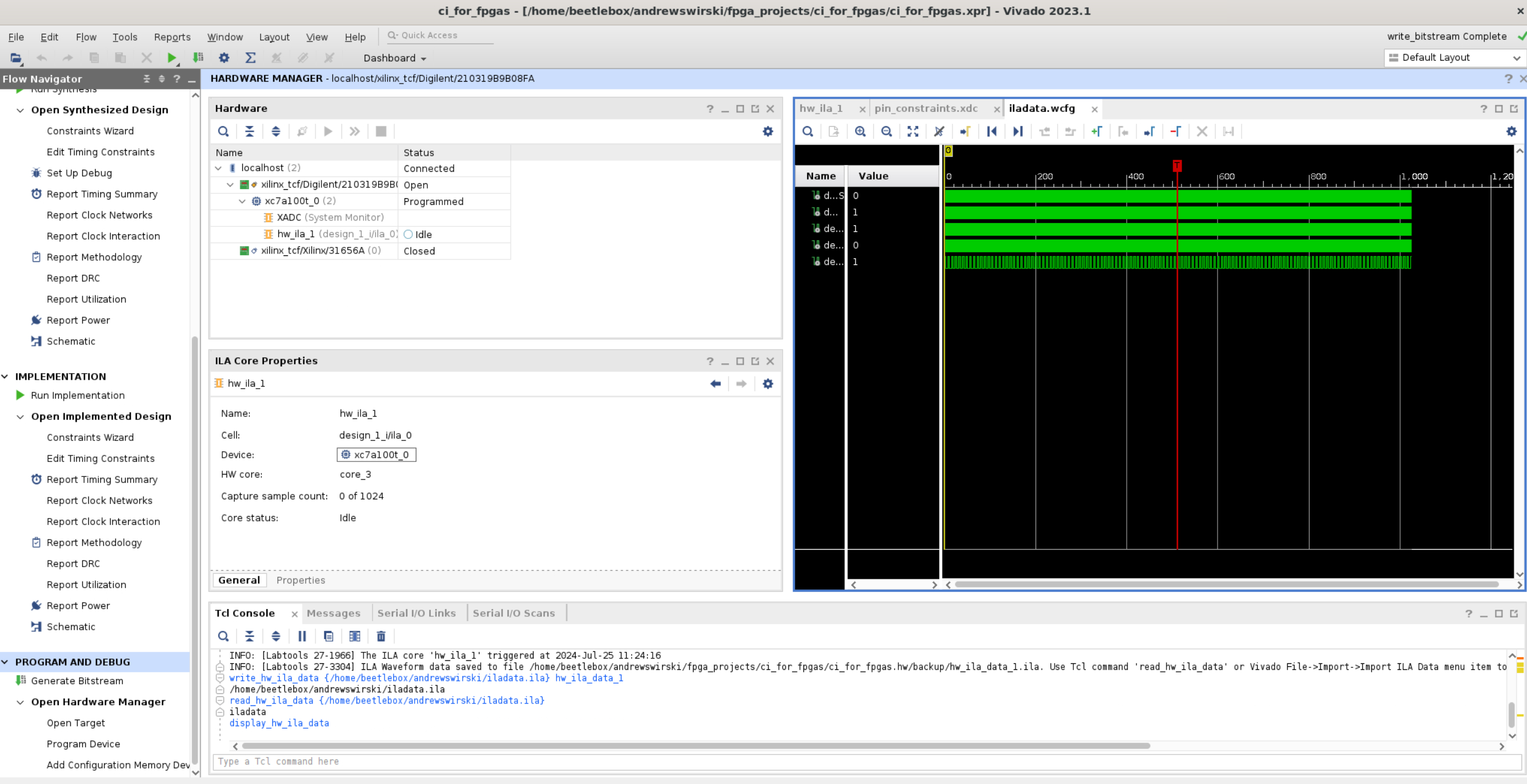
- In the downloaded folder, you should find
iladata.ila. Go back to Vivado and open this file by clicking back onto theHardware Managerand then going toFile > Import Data > Import ILA Data. This should contain your waveforms that are successfully running a full adder:
Conclusion
Congratulations, you have reached the end of this tutorial on getting started with AMD (Xilinx) FPGA. In this series you have learned:
- How to create a Vivado project and link it to a git repo.
- How to run simulation through continuous integration.
- How to use assertion statements to check for correctness in simulation.
- How to run synthesis, implementation and bitstream generation through continuous integration.
- How to trigger the ILA and extract the data through artifacts.
If you would like to learn more about BeetleboxCI please see our documentation or have a look at more of our tutorials.